The key features of the AXI protocol are:
The AXI protocol can provide many enhanced features, but the intent of this article is not to go into detail on the fancy features that most designers don’t need, but to concentrate on the normal interfaces that will suffice for most designs.
The current version of AXI is AXI4 which is widely supported by the FPGA vendors. But it should be noted that the Zynq-7000 actually supports AXI3 which is a subset of AXI4. The differences are minor, and the Xilinx tools automatically insert the necessary adaptation logic to translate between AXI3 and AXI4.
Operations on the AXI4 involve masters and slaves. Operations are initiated by a master and with the slave responding to the operation. Transfers on AXI can be initiated by either the master or the slave as described in the next section on channels.
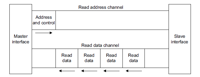
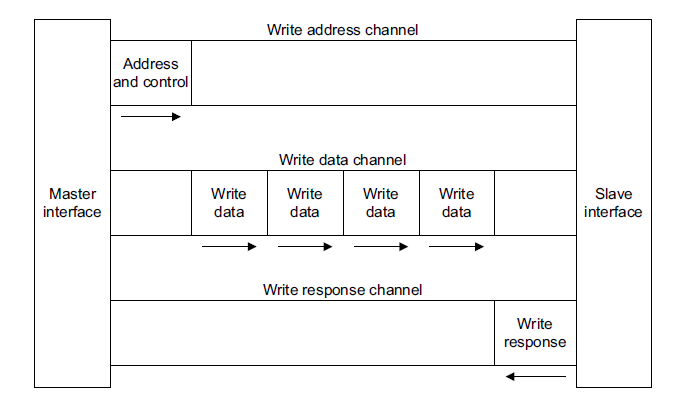
AXI communications take place in channels. Each channel is essentially a separate bus, but these channels are combined to facilitate what would normally be thought of as a single bus. For example, reads take place over the read address channel, sourced by the master, and the read data channel, sourced by the slave. Writes use three channels: the write address, write data, and write response channels. Having separate channels allows for concurrency, for example issuing read requests while the previously requested data is being returned. The following figure from the ARM AXI Specification illustrates the AXI4 Read Channel:

The master requests the read by providing the address, burst length, and other attributes on the read address channel, and the slave responds by sending the requested data on the read data channel. Each channel is like an individual bus with its own strobes.

The write address channel is essentially the same as the read address channel, validating the address, burst size, and other attributes of the cycle. Data is sent on the write data channel. Writes are considered buffered so that the master can perform writes without slave acknowledgement of the previous write. After the entire burst is complete, a single completion is sent from slave to master on the write response channel.
Like most synchronous interfaces today, AXI operates from a single clock. Although each channel can have a seperate clock as defined in the spec, this is also dependent upon the specific IP core. All interfaces include READY and VALID strobes which validate the transfer. Considering these signals from the perspective of the Write Data Channel, the slave issues READY when it is able to accept information (data, address, etc.) and the master issues VALID to validate information on the interface. Once the master issues VALID, it must remain asserted until at least the first the transfer occurs (READY high). A transfer takes place when both READY and VALID are high, so either side can generate wait states when desired. There is also a LAST signal which indicates the final data item on the interface.

In the above timing diagram, you can see the address is validated on the Write Address channel, and this is followed by the data on the Write Data channel. The slave responds with the status on the Write Response channel.
There are dependencies between the different channels, some defined in the AXI4 standard, and some defined by specific Xilinx IP modules.
The AXI4 protocol as defined is generic in that it doesn’t specify timing, allows for a wide variety of bus widths, and provides much flexibility in the type of transfers supported. For full AXI4, Xilinx supports data bus widths of 32 through 1024 in powers of 2. Burst lengths of up to 256 are supported. There are many features that aren’t of general interest, many of which aren’t supported by the Xilinx IP. Examples of such features as locked / exclusive access, protection/cache bits, quality of service, the low power interface, etc. These can easily be tied off to static values if one desires to interface to the full AXI4 – a requirement for bursting capabilities.

The AXI4 and AXI4 Lite protocols are memory mapped in that transactions always require an address. The AXI4 Streaming protocol removes that requirement. It is a data-centric protocol for bursting large amounts of data and includes much flexibility. Streaming signals can be identified as they are prepended with a “T”.
The streaming interface supports byte enables (the TKEEP strobe) and unaligned transfers (TSTRB strobe), and the same data handshake is used to transfer data: TVALID and TREADY. There is a TLAST strobe which can be used to indicate the end of transfer or other user defined termination condition. The TDEST signal can be used to indicate routing information from the source to the destination. It can also be used in conjunction with the identification field, TID.

Xilinx provides the AXI4 Interconnect IP core which can be used to manage AXI4 connections. The AXI Smartconnect is a newer version of the Interconnect core, though Xilinx recommends the Interconnect for lower performance applications (AXI4 Lite applications). These cores provide crossbar connectivity, support for multiple clock domains, FIFOs, width conversion, and protocol conversion. Note that these cores are used to connect AXI to AXI. If you are simply transferring data to the Zynq PS memory subsystem, then you may not need this.
Some of the features that this IP is useful for are: converting from full AXI4 to AXI4 Lite, gluing asynchronous clock domains together, fanning in multiple AXI4 interfaces to a single interface, or fanning out one to many.
Designing for the AXI protocol can take on different forms. When using the IP Integrator in Vivado, IPI takes care of most of the work for you. For the most part, you can simply configure and connect the models, but it helps to know what's going on behind the scene for high bandwidth connections.
If designing in HDL, it's a bit easier to design to the AXI4 Lite protocol than the full AXI4. But designing to full AXI4 really isn't as bad as one would think. It's true, there are many signals to deal with, but most of these are tied off to static values. One easy way to access these static values is to write out an example project from the IP Integrator.
For verification, there are bus functional models available. Originally, Xilinx provided an AXI Bus Functional Model (BFM), but this has been replaced by the AXI Verification IP. Here at Verien, we've developed our own which we use for our designs and can customize as needed to verify the design.