free html5 templates

© Copyright 2018 Verien Design Group, LLC  Concord, MA All Rights Reserved


Matlab/Simulink for FPGA Designs

This article discusses the use of Matlab / Simulink for FPGA designs, why one would want to use it and how to get started.


Why Use Matlab / Simulink for FPGA Designs?

There is much literature about the use of FPGAs for digital signal processing applications: the ability to run operations in parallel to achieve higher performance, or being able to run real time operations in a pipelined video or imaging system, or for applications which aren’t highly sequential in nature. But having made the decision to use an FPGA for your DSP, can’t it simply be created in HDL and simulation tested using a traditional digital simulator? The answer is yes, however for anything but the simplest of algorithms, one would be better off using Matlab / Simulink for reasons of simulation.

Simulink is a superior verification platform for DSP in FPGA. In the simulation testbench, one can drop down a few blocks to generate a sine wave or some other waveform, factor in some noise, vary the gain and offset with a couple more blocks and test at a higher rate, and hence for a longer period of time, than with a traditional digital simulator. The results implemented in Simulink are bit and cycle accurate which has some big advantages as are discussed below.

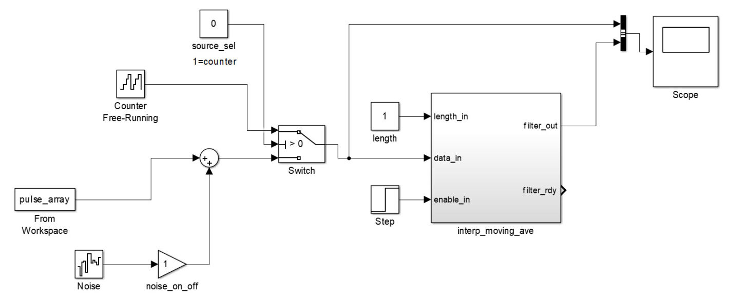
In the project below, you can see the block being developed in the interp_moving_ave block, which is instantiated in the testbench.  The testbench generates pulses from a file in the workspace (pulse_array) and we can optionally sum some noise into the data, if desired.  We also have the option to source a free-running counter into the input data, useful for testing boundary conditions.  

Simulink for FPGA Design


How to Design an FPGA Block using Matlab / Simulink

There are a couple of different options for capturing the design in Simulink. One is to use HDL Coder which is a Mathworks add-on tool, and the second is to use Xilinx System Generator for DSP, or as it is now called, Model Composer.
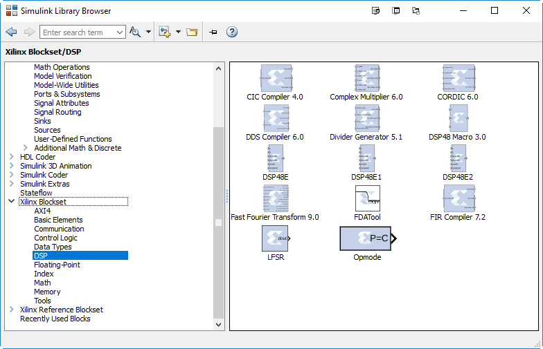
In Simulink, designs are captured graphically, similar to schematic design but at a high level. The components in Simulink are called “blocks” and the library that the blocks are referenced from is referred to as a “blockset”. Mathworks provides a normal Simulink blockset and many specialized blocksets for targeted applications. This blockset can be used with HDL Coder to generate synthesizable HDL from blocks captured in Simulink. The blocks need to be captured in a specific way; using the default floating point data type will not work for obvious reasons - you will generally need to be in fixed point in the FPGA. The alternative is to use the Xilinx tool called System Generator for DSP, or Sysgen. Sysgen includes a specialized blockset for FPGA designs. For users of Xilinx normal design flow, the blocks from the Sysgen blockset will look familiar – they are many of the same components found in Xilinx IP library: FIR filters, DDS, FIFOs, etc., along with some basic building blocks: adders, multipliers, logical operations, bit manipulation, and things like that.

Xilinx Simulink Blockset
FPGA Services


HDL Coder or System Generator / Model Composer?

Which is better, HDL Coder or System Generator / Model Composer? For the advanced Matlab / Simulink user who wants to target an FPGA, HDL Coder is probably the simpler choice as it allows the user to stay in their normal environment. However, I’ve found that System Generator (Model Composer) generates a more efficient design and makes better use of the specialized IP in the FPGA. This makes sense if you think about it, since it is using a tool created by Xilinx for Xilinx FPGAs.


Using System Generator / Model Composer

There are a few options when using Sysgen. For a simple algorithm, one can simply capture it directly in the Xilinx blockset and simulate using Simulink. But for a more complex algorithm, one is often better developing the algorithm in the Simulink blockset first. The blocks from the Simulink blockset default to floating point which will allow the designer to focus on the algorithm and not worry about precision to begin with.

Just as in an RTL design, there will be two parts to the simulation: the part that will be targeted into the FPGA – I’ll call this the model, and the part that will be used to simulation test this – the simulation testbench. Once the design is simulation tested, one approach is to copy over the model and connect it into the same simulation testbench. Then, one can go through the blocks in this copied model and convert them to fixed point, making all of the tradeoffs to deal with the growing precision that occurs. With both fixed and floating point models connected in the same testbench, one can perform the same simulations to gauge the error in converting to fixed point. It also a good practice to create simulations that test the boundary conditions and overflow – something that isn’t a concern in the floating point model, but could wreak havoc on the fixed point world.

After this step is complete, the next step is to convert the model to the Xilinx blockset.  There are just a few rules that need to be followed to capture a design with the Xilinx blockset: 
  1. The ports for the top level of the module have to pass through Gateway In (inputs) and Gateway Out (outputs) blocks.
  2. All block within the Gateway In and Gateway Out blocks must be from the Xilinx blockset.  
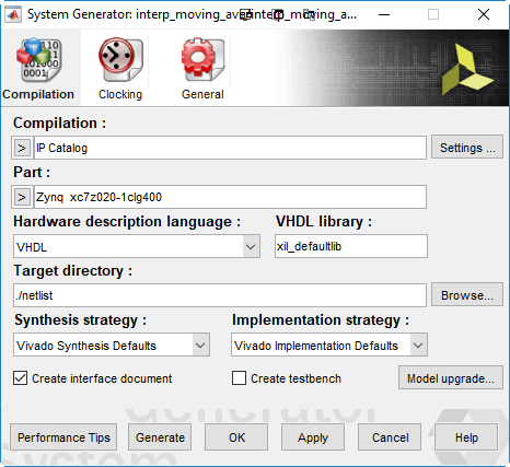
  3. The special System Generator block, or Model Composer Hub must be present somewhere in the design. This block is used to specify the parameters of the design: 
System Generator Block
Most of the blocks from the Xilinx blockset are configurable by double-clicking on them within Simulink. If you normally use HDL to capture your design, you’ll notice that the blocks in the Xilinx blockset look familiar – they are mostly the same blocks that can be built as cores using Vivado IP Integrator (Coregen under ISE).
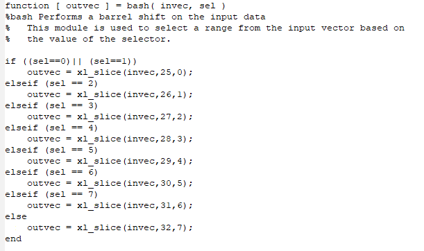
One unique block in the Xilinx blockset is the M-code block. This block allows you to use M-code to create either combinatorial or clocked functions in the native Matlab language. This is a bit different from HDL, but is pretty easy to get the hang of and is a bit easier to deal with than block based design, for some functions.
Simulink M-code


Getting the Model into the FPGA (Netlisting)

Once simulation is complete, the design can be brought into an HDL top level with just a few mouse clicks. Double click the System Generator block and specify IP Catalog along with a target directory. Clicking the generate button will generate a netlist. In Vivado, open up the IP Catalog and using a right mouse click, add the netlist folder that the model was compile into (not the IP catalog folder) to the catalog. Once in the IP catalog in Vivado, find the IP in the user repository and double click on it to add it to the project. The ports will be defined by the Gateway In and Out blocks that you added to the model. It’s generally a good idea to bring up a digital simulation of the model to make sure things went as planned, but since the model is bit and cycle accurate, there shouldn’t be any differences between the digital simulation and the Simulink simulation.
Resources

Tech Notes
IP Cores

Contact

Email: info@verien.com 
Phone: 978-405-3102 


© Copyright 2018 Verien Design Group, LLC Concord, MA All Rights Reserved